Please fill in the form below, so we can support you in your request.


    ASICAMD (Xilinx)AchronixIntel (Altera)LatticeMicrochip (MicroSemi)Other

    By submitting this form you are consenting to being contacted by the MLE via email and receiving marketing information.

    X
    CONTACT MLE
    Contact MLE for IP-Cores
    Please fill in the form below, so we can send you the relevant information regarding the IP-Cores of interest.


      Low-Latency 10G/25G Ethernet MACNPAP TCP/UDP/IP StackNVMe Streamer Gen3NVMe Streamer Gen4Key-Value StoreLinux PCIe FrameworkPCIe Long-Range TunnelPCIe NTBIBM OpenCAPISoft ADCSoft DACXilinx USB 2.0 EHCIXilinx XAUIXilinx RXAUIZynq Storage Exension

      By submitting this form you are consenting to being contacted by the MLE via email and receiving marketing information.

      X
      CONTACT MLE

      NVMe Streamer

      PCI Express (PCIe) Connectivity​

      NVMe Streamer

      NVMe IP Cores for Storage Acceleration

      NVMe (Non-Volatile Memory Express) has become the prominent choice for connecting Solid-State Drives (SSD) when storage read/write bandwidth is key. Electrically, the NVMe protocol operates on top of PCIe; it leaves behind legacy protocols such as AHCI, and thus scales well for performance. MLE has been integrating PCIe, and NVMe, into FPGA-based systems for a while. Now, MLE releases NVMe Streamer, an IP Core for NVMe Streaming, which is a so-called Full Accelerator NVMe host subsystem integrated into FPGAs, and most prominently into Xilinx Zynq Ultrascale+ MPSoC and RFSoC devices.

      MLE’s new NVMe Streamer is the result of many successful customer projects and responds to the embedded market’s needs to make use of modern SSDs. NVMe Streamer is a fully integrated and pre-validated subsystem stack operating the NVMe protocol fully in Programmable Logic (PL) with no software running, keeping the Processing System (PS) out of this performance path. For Xilinx FPGAs,  NVMe Streamer utilizes Xilinx GTH and GTY Multi-Gigabit Transceivers together with Xilinx PCIe Hard IP Cores for physical PCIe connectivity.

      Key Features

      • Provides one or more NVMe / PCIe host ports for NVMe SSD connectivity
      • Full Acceleration means “CPU-less” operation
      • Fully integrated and tested NVMe Host Controller IP Core
      • PCIe Enumeration, NVMe Initialization & Identify, Queue Management
      • Control & Status interface for IO commands and drive administration
      • Approx. 50k LUTs and 170 BRAM tiles (for Xilinx UltraScale+)
      • Compatible with PCIe Gen 1 (2.5 GT/sec), Gen 2 (5 GT/sec), Gen 3 (8 GT/sec), Gen 4 (16 GT/sec) speeds
      • Scalable to PCIe x1, x2, x4, x8 lane
      NVMe IP - NVMe Streamer Block diagram

      Applications

      • High-speed analog and digital data acquisition
      • Lossless and gapless recording of sensor data
      • Automotive / Aerospace Data Logging
      • Data streaming from SSDs
      • Storage protocol offloading

      Evaluation System for NVMe Streamer (NVMe IP)

      new_64px
      AMD Versal™ AI Edge Evalboard from Trenz

      TE0950 AMD Versal™ AI Edge Evalboard from Trenz Electronic

      NVMe IP Core - NVMe Streamer Evaluation System - FPGADrive

      NVMe IP Core - NVMe Streamer Evaluation System - Zynq UltraScale+ MPSoC ZCU106

      Zynq UltraScale+ MPSoC Evaluation System

      In collaboration with FPGA ecosystem partner Opsero, MLE provides an evaluation system based on Opsero’s FPGADrive.


      NVMe IP Core - NVMe Streamer Evaluation System - FPGADrive


      Pricing

      MLE’s license fee structure reflects the needs for simple and affordable NVMe IP Core for connectivity:

      Product Name  Deliverables Example Pricing

      Evaluation Reference Design 

      (NVMe Streamer ERD)

      Binary-only system stack compiled under Vivado Tried and tested to work on the Xilinx ZCU106 Development Kit. Evaluation-only license, valid for 30 days.

      free of charge

      Production Reference Design – Professional Edition

      (NVMe Streamer PRD-PE)

      Complete, downloadable NVMe Host and Full Accelerator subsystem integrated into the ERD example system. Delivered as Vivado design project with encrypted RTL code. Production-ready: Pre-integrated and tested to be portable to Your target system hardware. Fully paid-up for, royalty-free, world-wide, Single-Project-Use License, synthesizable for 1 year. Up to 40 hours of premium support, customization and/or integration design services via email, phone or online collaboration.

       starting at $24,800.-

      Inquire

      Application / Project specific Expert Design Services

      System-level design, modeling, implementation and test for realizing Domain-Specific NVMe Streaming / Recording Architeture.

      $1,480.- per engineering day 

      Documentation

      Frequently Asked Questions​

      No, NVMe Streamer is so-called Block Storage. So, no file systems are not supported. For each data transfer the user application logic selects a start and maximum end address, and then data is written to flash in a linear fashion. This achieves best performance and avoids write amplifications.

      Partitions are not explicitly supported. However, the user application logic can use NVMe Streamer to read the SSD’s partition table and then set up transfers with start and maximum end address to be aligned to partitions.

      Only one single namespace is supported.

      The standard for NVMe Streamer is to be directly connected to one single NVMe SSD where the FPGA acts as a so-called PCIe Root Complex and the SSD acts as the so-called PCIe Endpoint. However, we can customize NVMe Streamer for your application to support more complex PCIe topologies, including multiple direct-attached SSDs, multiple SSDs connected via a 3rd party PCIe switch chip, or even PCIe Peer-to-Peer. Please ask us for more details.

      NVMe Streamer currently supports one single IO Queue. This IO Queue can have up to 128 entries, each with up to 128 KiB data. I.e. you can have up to 16 MiB of “data in flight”. If needed, we can change the depth and size of this IO Queue. However, given the needs of streaming applications increasing the number of IO Queues may not be advantageous.

      Yes, this is supported in a customized configuration. Peer-to-Peer transfers can be very attractive as it frees up the host CPU. Team MLE can customize NVMe Streamer for your application to support many more complex PCIe topologies, including multiple direct-attached SSDs, multiple SSDs connected via a 3rd party PCIe switch chip, including PCIe Peer-to-Peer. Please ask us for more details.

      NVMe Streamer can be configured via an AXI4-Lite register space. This register space is also used to set up and control streaming transfers. The actual data exchange then is handled via an AXI4-Stream master and slave. Some GPIO style status signals for informational purposes, like LEDs, are provided as well. This is documented in our developers guide.

      Currently, only one single stream of data is supported by NVMe Streamer. Therefore, it is the designer’s responsibility to buffer additional streams and provide said streams to NVMe Streamer once the active stream is finished. An alternative can be to multiplex streams while writing to flash. The latter works well, for example, for multiple ADC inputs with same sample rate and width.

      Yes. Because NVMe Streamer is agnostic to the formfactor of your SSD m.2, EDSFF and so on are supported, as long as your SSD “speaks the NVMe protocol” and not SATA nor SAS.

      While, again, NVMe Streamer is compatible to work with any NVMe SSD, there are a couple of other aspects to keep in mind when selecting an NVMe SSD: Noise, vibration, harshness, temperature throttling, local RAM buffers, SLC, MLC, TLC, QLC, 3D-XPoint, etc. To enable our customers to deliver dependable performance solutions, we have worked with a set of 3rd party SSD vendors and would be happy to give you technical guidance in your project. Please inquire.

      Low-Latency Ethernet MAC

      Low-Latency Ethernet MAC

      Low Latency Ethernet

      10G/25G MAC IP

      Low Latency Ethernet MAC IP

      The German Fraunhofer Heinrich-Hertz-Institute (HHI) partners with MLE to commmercialize and market HHI’s proven network technology solutions.  The Low Latency Media Access Controller (MAC) IP Core for 10G/25G Ethernet enables high-bandwidth, low latency Ethernet communication solutions for FPGA-based systems at 10 Gbps or 25 Gbps line rate. 

      MLE is a licensee of Fraunhofer HHI, and offers a range of technology services, sublicenses and business models compatible with customer’s ASIC or FPGA project settings, world-wide.

      Key Features

      • Platform and device vendor independent core
      • Supports 10G or 25G Ethernet
      • Low Latency, 19.2ns at 64-Bit at 156.25MHz
      • AXI4-Stream protocol support on client transmit and receive interface
      • Low resource usage
      • Deficit Idle Count mechanism to ensure full data rate
      • Padding of short frames (<64 byte)
      • Support for VLAN tagged frames
      • Promiscuous mode support
      • Generation and checking of CRC-32 at full line rate
      • Optional user defined maximum frame length up to 64 kb or complete disabling of frame length check
      • Customization through configuration vector to trade resources for functionality
      Low Latency Ethernet 10G/25G MAC FPGA IP

      Pricing

      The Low Latency Ethernet 10G/25G MAC is available as a combination of Intellectual Property (IP) Cores, reference designs, plus supporting design integration services:

       Product Name  Deliverables Example Pricing

      Intellectual Property (IP) Cores

      Fully paid-up-for Single-Project or Multi-Project Use IP Core license for FPGA; delivered as encrypted netlist or RTL.

      starting at $9,800.-

      Inquire

      Documentation

      Fraunhofer HHI

      Founded in 1949, the German Fraunhofer-Gesellschaft undertakes applied research of direct utility to private and public enterprise and of wide benefit to society. With a workforce of over 23,000, the Fraunhofer-Gesellschaft is Europe’s biggest organization for applied research, and currently operates a total of 67 institutes and research units. The organization’s core task is to carry out research of practical utility in close cooperation with its customers from industry and the public sector.

      Fraunhofer HHI was founded in 1928 as “Heinrich-Hertz-Institut für Schwingungsforschung“ and joined in 2003 the Fraunhofer-Gesellschaft as the “Fraunhofer Institute for Telecommunications, Heinrich-Hertz-Institut„. Today it is the leading research institute for networking and telecommunications technology, “Driving the Gigabit Society” .

      NPAP FPGA TCP/UDP/IP Stack

      FPGA TCP/UPD/IP - Network Protocol Accelerator Platform (NPAP)

      TCP/UDP/IP Network Protocol 

      Accelerator Platform (NPAP)

      Accelerate Network Protocols with FPGA TCP/UDP/IP Stack

      The German Fraunhofer Heinrich-Hertz-Institute (HHI) has partnered with MLE to market the proven network accelerators “TCP/IP & UDP Network Protocol Accelerator Platform (NPAP)”.  This customizable solution enables high-bandwidth, low-latency communication solutions for FPGA- and ASIC-based systems for 1G / 2.5G / 5G / 10G / 25G / 40G / 50G / 100G Ethernet links.

      MLE is a licensee of Fraunhofer HHI, and offers a range of technology services, sublicenses and business models compatible with customer’s ASIC or FPGA project settings, world-wide.

      If you are interested in optimizing your Linux based system for best performance with NPAP, we do suggest to read this technical publication from Bruno Leitao, IBM: “Tuning 10Gb network cards on Linux“.

      Core Benefits

      • Accelerate CPUs by offloading TCP/UDP/IP processing into programmable logic (“Offloading”)
      • Increase network throughput and reduce transport latency
      • Bring full TCP/UDP/IP connectivity to FPGAs even if no CPU available (“Full Acceleration”)
      • Complete and customizable turn-key solutions and IP cores based on the TCP/UDP/IP stack from the Fraunhofer HHI
      • All MAC / Ethernet / IPv4 / UDP / TCP processing is implemented in HDL code, synthesizable to modern FPGAs and ASIC
      • User applications can either be implemented in FPGA logic or in software via application-specific interfaces to CPUs

      Key Features

      • Highly modular TCP/UDP/IP stack implementation in synthesizable HDL
      • Full line rate of 70 Gbps or more in FPGA, 100 Gbps or more in ASIC
      • 128-bit wide bi-directional data paths with streaming interfaces
      • Multiple, parallel TCP engines for scalable processing
      • Network Interface Card functionality with Bypass (optional)
      • DPDK Stream interface (optional)
      • Corundum NIC integration with performance DMA and PCIe (optional)

      Applications

      • FPGA-based SmartNICs
      • In-Network Compute Acceleration (INCA)
      • Hardware-only implementation of TCP/IP in FPGA
      • PCIe Long Range Extension
      • Networked storage, such as iSCSI
      • Test & Measurement connectivity
      • Automotive backbone connectivity based on open standards
      • Video-over-IP for 3G / 6G / 12G transports
      • Increase throughput for 10G/25G/50G/100G Ethernet
      • Reduce latency in System-of-Systems communication

      Remote Evaluation System for Network Protocol Accelerator Platform (NPAP)

      Try out the Network Protocol Accelerator Platform (NPAP) using MLE’s Remote Evaluation System which lets you connect to MLE’s IP core evaluation lab via a remote connection so you can evaluate and try out this IP core from MLE and partners.

      • Evaluate and try the IP core when it is running live on an FPGA system under your control – which saves you from engineering time to integrate and compile the IP core on target hardware
      • Have your own copy of a virtual environment – which allows you to run your tests, keep your logs, for example, if your calendar forces you to interrupt your current evaluation
      FPGA TCP/UPD/IP Network Accelerators - Network Protocol Accelerator Platform (NPAP) remote evaluation in 10G

      This remote evaluation is based on the NPAP-10G Evaluation Reference Design (ERD) for Xilinx Zynq UltraScale+ MPSoC running on the ZCU102 DevKit. The ZCU102 Devkit is physically connect via a 10GigE Twinax cable to a Mellanox ConnectX-4 LX 10G/25G NIC which sits inside the host running Your VM.

      Below are the FPGA-based solutions currently supported by MLE’s Evaluation Reference Designs (ERD) for NPAP:

      AMD Versal™ AI Edge Evalboard from Trenz
      MLE NPAC-40G SmartNIC Board - FPGA TCP/UDP/IP Network Accelerator
      • Targeted to Intel Stratix 10 GX 400
      • Netperf and TCP-/UDP-Loopback example instances
      • 4x SFP+ for 4x 10 GigE via Twinax or Fibre
      • Supports Quartus design flow with High-Level Synthesis design option
      • Runs on MLE NPAC-40G Cost-Optimized SmartNIC
      AMD/Xilinx ZCU111 Zynq Ultrascale+ RFSoC Development Kit - FPGA TCP/UDP/IP Network Accelerator
      • Targeted to Xilinx Zynq Ultrascale+ RFSoC ZU28DR (see Eval Guide)
      • Quad-Core ARM A53MP runs Xilinx PetaLinux
      • Netperf and TCP-/UDP-Loopback example instances
      • SFP28 for 25 GigE via Twinax or Fibre
      • Supports Vivado design flow with High-Level Synthesis design option
      • Runs on Xilinx ZCU111 Development Kit
      AMD/XIlinx ZCU102
      • Targeted to Xilinx Zynq Ultrascale+ MPSoC ZU9 (see Eval Guide)
      • Quad-Core ARM A53MP runs Xilinx PetaLinux
      • Netperf and TCP-/UDP-Loopback example instances
      • SFP+ for 10GigE via Twinax or Fibre
      • Supports Vivado design flow with High-Level Synthesis design option
      • Runs on Xilinx ZCU102 Development Kit
      AMD_Xilinx Alveo U200 Data Center Accelerator Card
      • Targeted to AMD/Xilinx UltraScale+ FPGA
      • Netperf and TCP-/UDP-Loopback example instances
      • QSFP28 for 4x 25 GigE via Twinax or Fibre
      • Supports Vivado design flow with High-Level Synthesis design option
      • Runs on Alveo U200 complemented by AMD OpenNIC FPGA Shell and device drivers
      Intel FPGA SmartNIC N6000-PL Platform
      • Targeted to Intel Agilex AGF014 F Series FPGA
      • Netperf and TCP-/UDP-Loopback example instances
      • QSFP28 for 4x 25 GigE
      • Supports Quartus design flow with High-Level Synthesis design option
      • Runs on Intel FPGA SmartNIC N6000-PL Platform
      Intel Stratix 10 GX Development Kit
      • Targeted to Intel Stratix 10 GX (see Eval Guide)
      • Netperf and TCP-/UDP-Loopback example instances
      • SFP+ for 10 GigE via Twinax or Fibre
      • Supports Quartus design flow with High-Level Synthesis design option
      • Runs on Intel Stratix 10 GX Development Kit
      Intel Cyclone 10 GX Development Kit
      • Targeted to Intel Cyclone 10 GX (see Eval Guide)
      • Netperf and TCP-/UDP-Loopback example instances
      • SFP+ for 10 GigE via Twinax or Fibre
      • Supports Quartus design flow with High-Level Synthesis design option
      • Runs on Intel Cyclone 10 GX Development Kit
      Microsemi PolarFire MPF300-EVAL-KIT
      • Targeted to Microsemi PolarFire (see Eval Guide)
      • Netperf and TCP-/UDP-Loopback example instances
      • SFP+ for 10 GigE via Twinax or Fibre
      • Supports Libero design flow with High-Level Synthesis design option
      • Runs on Microsemi PolarFire MPF300-EVAL-KIT

      Pricing

      MLE’s Network accelerators – Network Protocol Accelerator Platform (NPAP) – is available as a combination of Intellectual Property (IP) Cores, reference designs, and design integration services:

      Product Name Deliverables Example Pricing
      Network Processing Device Integrated processing device solution, built on top of leading FPGA technology, encapsulating one or more Network Protocol Accelerators for 1GbE and/or 10GbE.

      Based on NRE and unit volume 

      Inquire

      Intellectual Property (IP) Cores Single-Project or Multi-Project Use; ASIC or FPGA; Modular and application-specific IP cores, and example design projects; delivered as encrypted netlists or RTL. starting at $78,000.-
      (depends on FPGA device and line rate, please inquire)
      Evaluation Reference Design (ERD) Available upon request as FPGA design project, with optional customizations (different target device, different transceivers, etc) free-of-charge
      Application-specific R&D Services Advanced network protocol acceleration R&D services with access to acceleration experts from Fraunhofer HHI and/or MLE. $1,680.- per engineering day 

      Documentation

      Encrypted Network Acceleration Solutions (ENAS)

      TCP-TLS 1.3 for Secure 10/25/50 GigE

      ENAS are joint solutions of MLE’s TCP/IP Network Protocol Accelerator Platform (NPAP) and Xiphera’s Transport Layer Security (TLS) 1.3 to ensure secure and reliable connection between devices over LAN and WAN. It implements Transport Layer Security, a cryptographic protocol that provides end-to-end data security, on top of the Transmission Control Protocol (TCP) layer.

      Frequently Asked Questions

      NPAP is integrated with the FPGA vendors PCS/PMA layer and thus is compatible with other IEEE compliant Ethernet Network Interface Cards (NIC) for 1 GigE, 10 GigE, 25 GigE, 40 GigE, 50 GigE, 100 GigE. Please refer to the FPGA device vendors documentation of the subsystem for further information.

      NPAP implements all networking functions required by IETF RFC 1122 and thus is interoprable with software stacks from Microsoft Windows, Open-Source Linux (3.x or newer) as well as Mellanox/libvma or SolarFlare OpenOnload. Please refer to the NPAP Datasheet for more information.

      Yes, typically, we configure and instantiate NPAP with BRAMs for the Rx/Tx buffers. For applications where NPAP transmits data to a server we suggest 128K Bytes per TCP session (i.e. TCP port instance) to accomodate the (slower) processing of the software TCP stack running on the Recipient. Please refer to the NPAP Datasheet for more information.

      Here is the metric to determine TCP buffer sizes for NPAP (keep in mind, that TCP buffers are placed on both ends: Tx side and Rx side):

      Buffer size (in bits) = Bandwidth (in bits-per-second) * RTT (in seconds)

      RTT is the Round-Trip Time which is the time for the Sender to transmit the data plus the time-of-flight for the data, plus the time it takes the Recipient to check for packet correctness (CRC), plus the time for the Recipient to send out the ACK, plus the time-of-flight for the ACK, plus the time it takes the Sender to process the ACK and release the buffer.

      For example:

      1. If the recipient is NPAP in a direct connection then we can assume ACK times less than 20 microseconds, i.e. buffer sizes shall be 200k bits. Means in this case a 32 kBytes on-chip BlockRAM per TCP session will be sufficient.
      2. If the recipient is software then RTT can be much longer, mostly due to the longer processing times in the OS on the recipient side. For a modern Linux we can assume RTT of 100 microseconds, or longer (see here [1] or run a ‘ping localhost’ on your machine). Means buffer sizes shall be around 1M bits, or the 128K Bytes of BRAM we typically instantiate.

      Fraunhofer HHI

      Founded in 1949, the German Fraunhofer-Gesellschaft undertakes applied research of direct utility to private and public enterprise and of wide benefit to society. With a workforce of over 23,000, the Fraunhofer-Gesellschaft is Europe’s biggest organization for applied research, and currently operates a total of 67 institutes and research units. The organization’s core task is to carry out research of practical utility in close cooperation with its customers from industry and the public sector.

      Fraunhofer HHI was founded in 1928 as “Heinrich-Hertz-Institut für Schwingungsforschung“ and joined in 2003 the Fraunhofer-Gesellschaft as the “Fraunhofer Institute for Telecommunications, Heinrich-Hertz-Institut„. Today it is the leading research institute for networking and telecommunications technology, “Driving the Gigabit Society” .

      IP-Cores

      FPGA IP Cores & Licensable Subsystem Stacks

      ASIC / FPGA IP Cores & Licensable Subsystem Stacks

      An intellectual property core (IP core), or so-called IP block, is a reusable unit of logic or integrated circuit layout design. MLE offers various pre-validated ASIC / FPGA IP cores and custom services for Network Acceleration, Storage Acceleration, PCIe Non-Transparent Bridge (PCIe NTB), AMD/Xilinx legacy devices, and Mixed-Signal applications.

      Network Acceleration

      Network Acceleration FPGA IP Cores

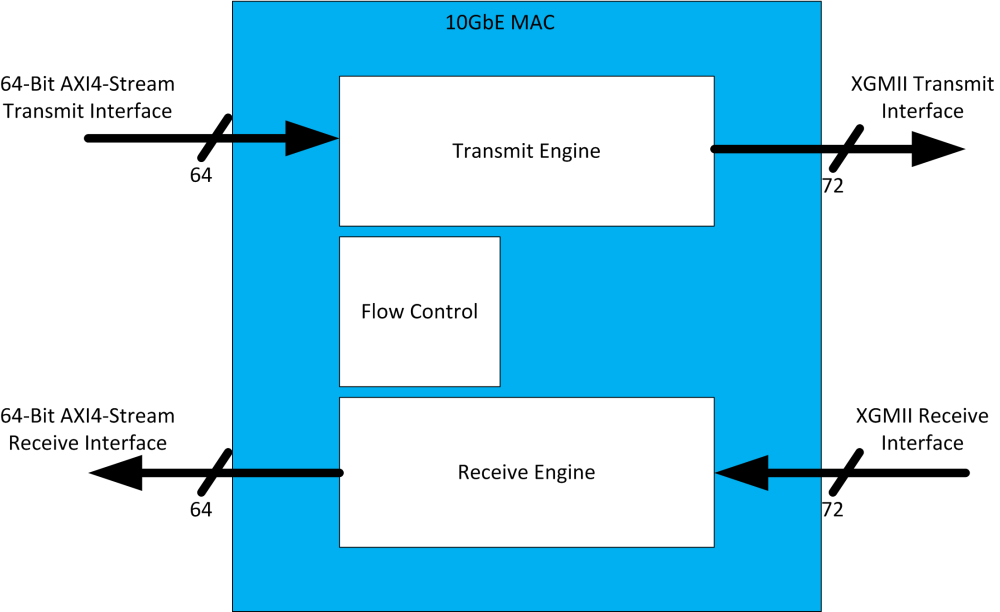
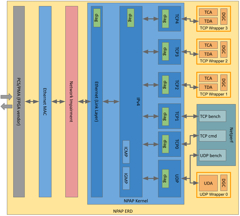
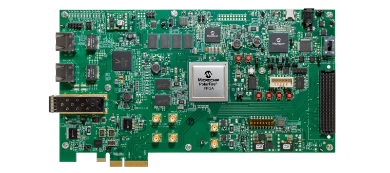
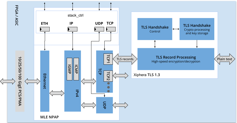
      MLE’s network acceleration ASIC / FPGA IP cores with patented and patent pending technology provides distinct advantages for offloading and accelerating network protocol processing at speeds up to 100 Gbps in FPGA, or faster in ASIC.

      Storage Acceleration

      Storage Acceleration FPGA IP Cores

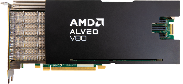
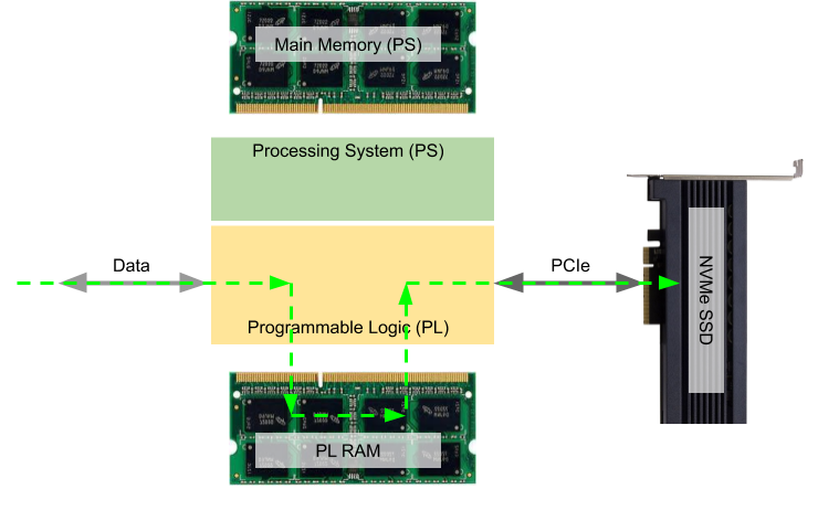
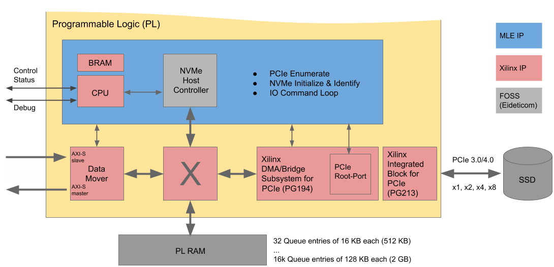
      Next-generation storage protocols such as NVMExpress (NVMe) provide significant performance benefits and, when combined with FPGAs, can be used as storage acceleration IP cores for Computational Storage, Data-in-Motion processing and high-speed data capture and recording.

      PCI Express

      PCI Express FPGA IP Cores 
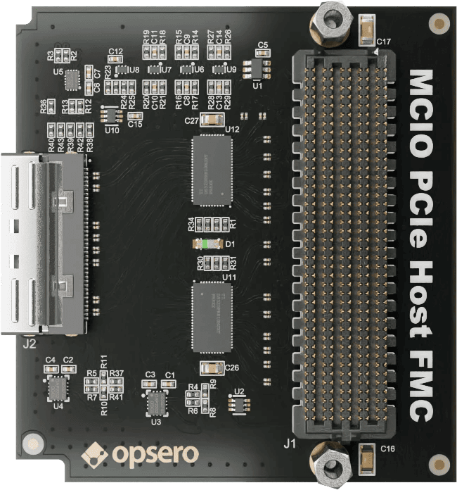
MLE provides complete system stacks and IP cores for PCIe Connectivity between FPGAs, CPUs, GPUs and SoCs, which allow implementation of high-performance, low-latency data transfers without expert knowledge of PCIe. Our patented and patent pending technology can be used for PCIe direct connect or Long-Range Tunneling and supports topologies from PCIe point-to-point to networks using Non-Transparent Bridging.

      Xilinx Long-term Support

      Xilinx FPGA IP Long-term Support
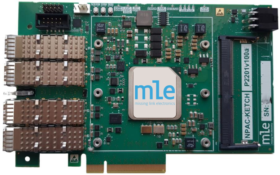
Xilinx has selected MLE to provide long-term support for discontinued IP Cores including XPS USB 2.0 EHCI Host Controller and the XAUI and RXAUI IP Cores for Xilinx devices.

      Mixed-Signal FPGA

      Mixed-Signal FPGA

      MLE’s patented technology enables Mixed-Signal FPGA solutions based on integrate Delta-Sigma converters in FPGA logic and LVDS FPGA pins to reduce BoM costs and PCB footprint.

      FPGA Design Services

      FPGA Design Services

      MLE’s engineering team takes a system-level view, has special expertise and has been equipped by leading FPGA vendors to de-risk your next FPGA design project.