NVMe Fast FPGA RAID Accelerator
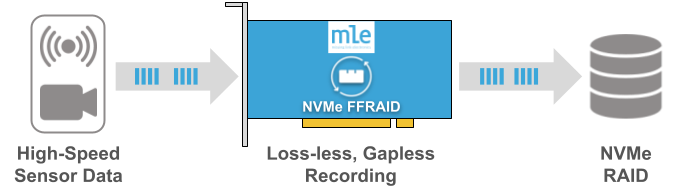
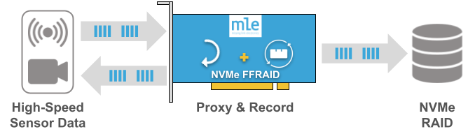
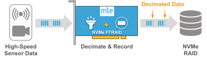
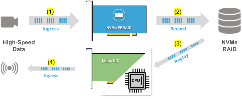
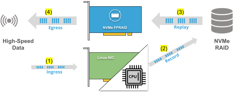
 Data Recorder Application Scenario")


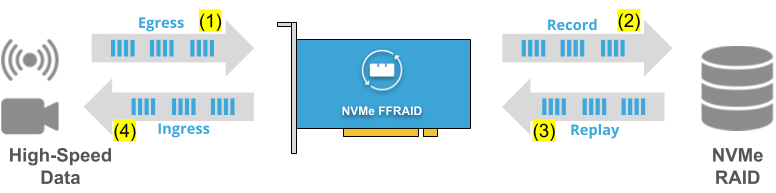
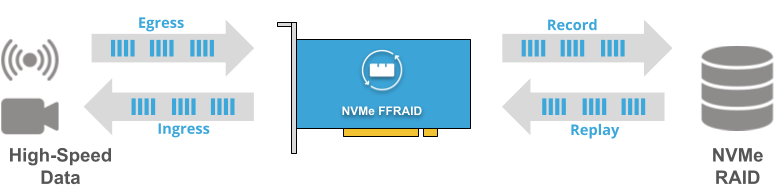
 Turnkey System")


Xiphera Ltd.
![]()
Xiphera, Ltd, is a Finnish company designing hardware-based security solutions using standardised cryptographic algorithms. We have strong cryptographic expertise, extensive experience in system design, and deep knowledge on reprogrammable logic, enabling us to protect our customers’ critical information and assets.
Xiphera’s product portfolio consists of secure and efficient cryptographic Intellectual Property (IP) cores, designed directly for Field Programmable Gate Arrays (FPGAs) and Application Specific Integrated Circuits (ASICs). Our widely applicable solutions for various end markets offer our customers peace of mind in a dangerous world.


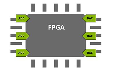
| Standard Approach | MLE Mixed Signal FPGAs |
|---|---|
|
|


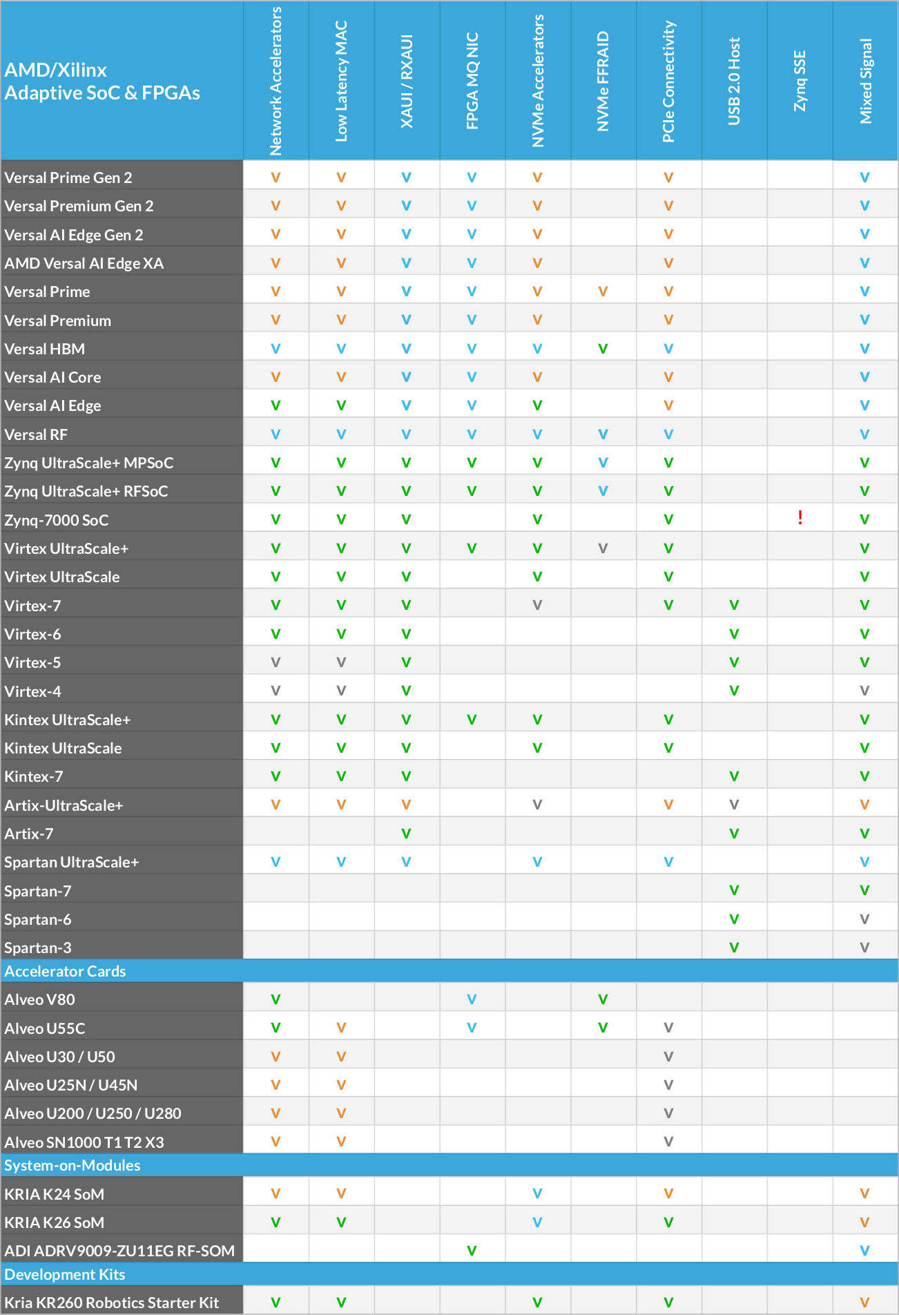
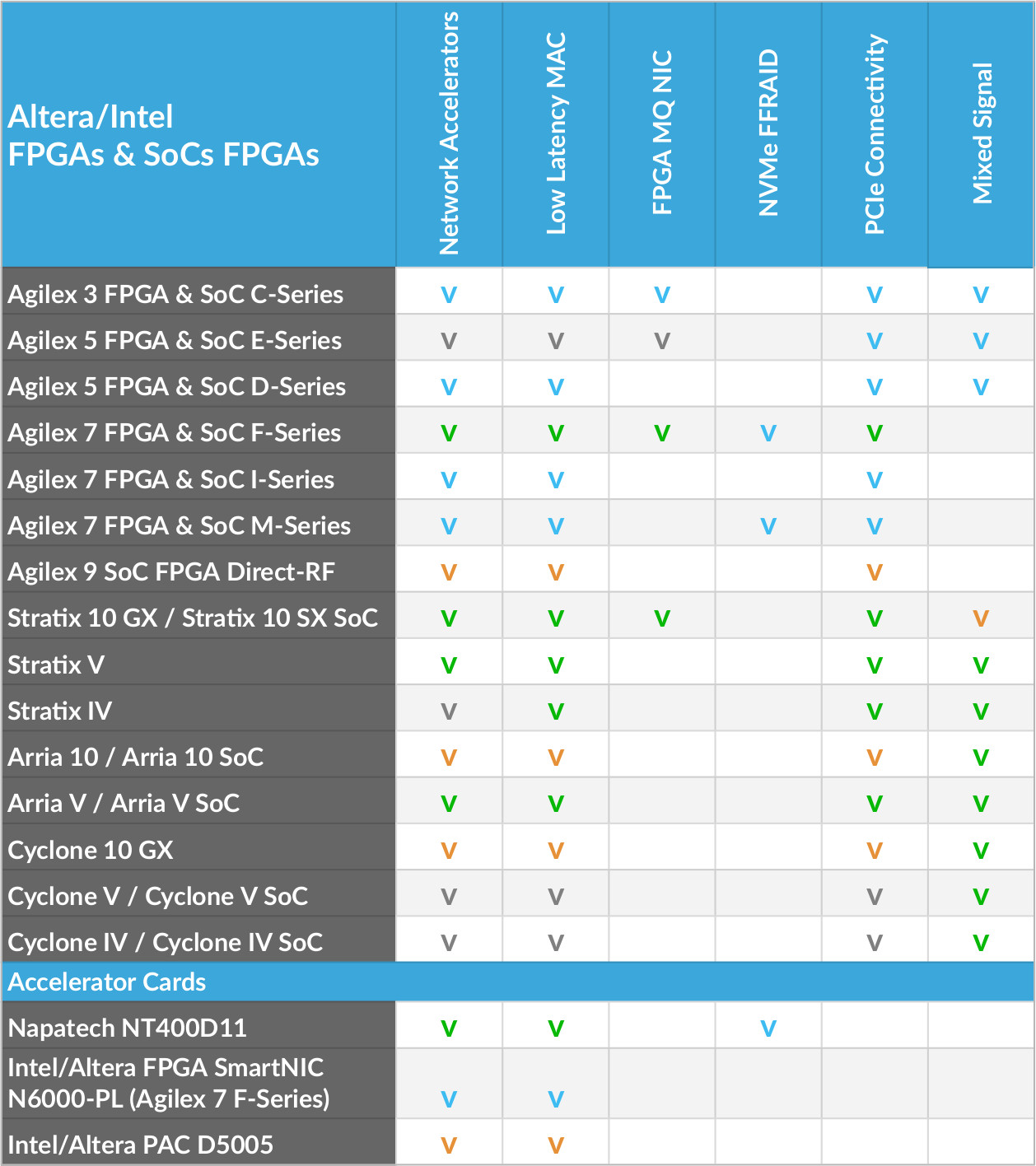
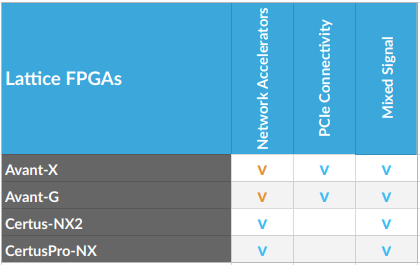
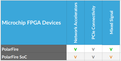
MLE develops a close partnership with the key FPGA vendors and support a wide range of FPGA devices from AMD, Intel, Lattice and Microchip for custom IP core design. The tables below high-light MLE Product Support as of Oct, 2025:
| Legend | |
| v | Fully supported |
| v | Supported with restrictions |
| v | Supported, in development |
| v | Support on Product Roadmap |
| ! | Not recommended for new designs |
| Not Applicable / no supported | |
Looking for a specific FPGA for IP Core Design Service?
Contact Us