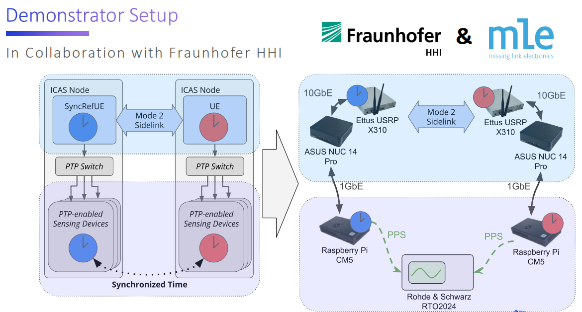
GNSS is widely used for positioning and synchronization—particularly in applications, such as vehicles and drones, where merging recorded radar data and coordinating multiple nodes over-the-air is essential. Accurate time-stamping is crucial to ensure data integrity, which requires a reliable and common time source. However, GNSS connectivity can be limited or completely unavailable in challenging environments like tunnels or urban canyons, making precise synchronization difficult.
In this presentation, MLE showcases our approach to synchronize devices using PTP-based application layer time synchronization over 5G sidelink. We walk through the approach and implications of correlating PTP messages with 5G PHY layer frame timing, and briefly touch on a method for further improving the timestamp accuracy. In the end, we present our proof-of-concept demonstrator setup developed in collaboration with Fraunhofer HHI, along with initial experimental results, demonstrating microsecond-level time synchronization accuracy via PTP over 5G sidelink. Notably, this approach relies purely on existing mechanisms and requires no additional modifications to future 6G standards.
In the decade of high-performance networking and computing, FPGAs have arisen as a promising and highly convenient solution, offering flexibility, reprogramming capacity and parallelism options. The role of high-performance solutions that offer a high throughput in network-related operations is extremely beneficial in real-time processing tasks executed on embedded systems, such as real-time video streaming.
This presentation showcases the capabilities and obtained performance of our FPGA-based high-speed multi GMSL camera to RTP streaming solution using a single 10GbE link. There will be a walk through the multi GMSL Ser/Des integration, and the FPGA-powered components overview: the CSI-2 to RTP streams translation and the multi-GMSL camera synchronization, accompanied by the highly configurable and low-latency UDP/IP network accelerator. The described high-performance data path is integrated with the on-chip CPU subsystem to provide time synchronization via PTPv2 and enable control and monitoring of the device via the network. At the end of the presentation, we emphasize the most important design choices to build such a multi-camera streaming system. We finally draw the conclusions and the lessons learned from that successful experience.
Date: Thursday July 3rd, 2025
Track 2 – Embedded / Vision (starts at 1:30pm CEST)
Location: Hotel NH München Ost Conference Center, Munich, Germany
Join MLE and Analog Devices at FPGA Conference 2025 to discover how we built the highly configurable and low-latency Multi GMSL Camera for 10GbE RTP Streaming!
Enter the promo code FPGA25-CON-MEETME to get 20% discount on all tickets!
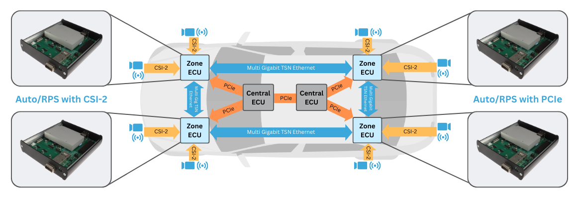
Automotive architectures are transforming: while more and more sensors become integrated in vehicles, the automotive industry is looking for ways to reduce wiring efforts in production, more scalability, higher level of integration and faster ways development.
Auto/TSN stands for automotive data over Time-Sensitive Networks which is an in-vehicle network infrastructure based on open standards such as IEEE Ethernet.
Auto/TSN virtualizes the in-vehicle network infrastructure: Key objective is to reduce costs, increase scalability and enable upgradability for next-generation automotive architectures including electric and/or autonomous vehicles.
The presentation will show how a zone based architecture can look like in comparison to the “classic” wiring. It will explain the tasks of a zone gateway and why FPGA/Soc play a major role in sensor fusion. Further more why it is important to use middleware which turns devices in a service for a central car server and other ECUs. For visualization, we will show examples of the government funded CeCaS research project and show the complete chain from camera sensors over zone gateways to the central car server.
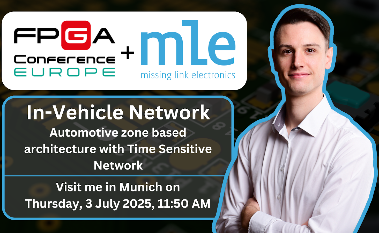
Date: Thursday July 3rd, 2025
Track 1 – Application (starts at 11:50am CEST)
Location: Hotel NH München Ost Conference Center, Munich, Germany
Join us at FPGA Conference 2025 to learn more details about the automotive zone-based architecture with TSN technology!
Enter the promo code FPGA25-CON-MEETME to get 20% discount on all tickets!
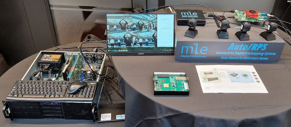
For the AMD Technology Day in Gothenburg, Sweden, MLE presented an automotive rapid prototyping system for architecture exploration and development of future Zone based automotive architectures. The outcome presented based on a practical example of work done in the MANNHEIM CeCaS Project.
The national funded research project MANNHEIM CeCaS (Central Car Server) was initiated between industry and academia, focusing on the creation of fundamental hardware and software building blocks for next-generation automotive technology. Key innovations span from chip technology & HW acceleration, E/E architecture & topology, to networking & communication, software architecture & abstraction, housing & cooling, as well as methodologies like AI-based system modelling and HW/SW co-design.
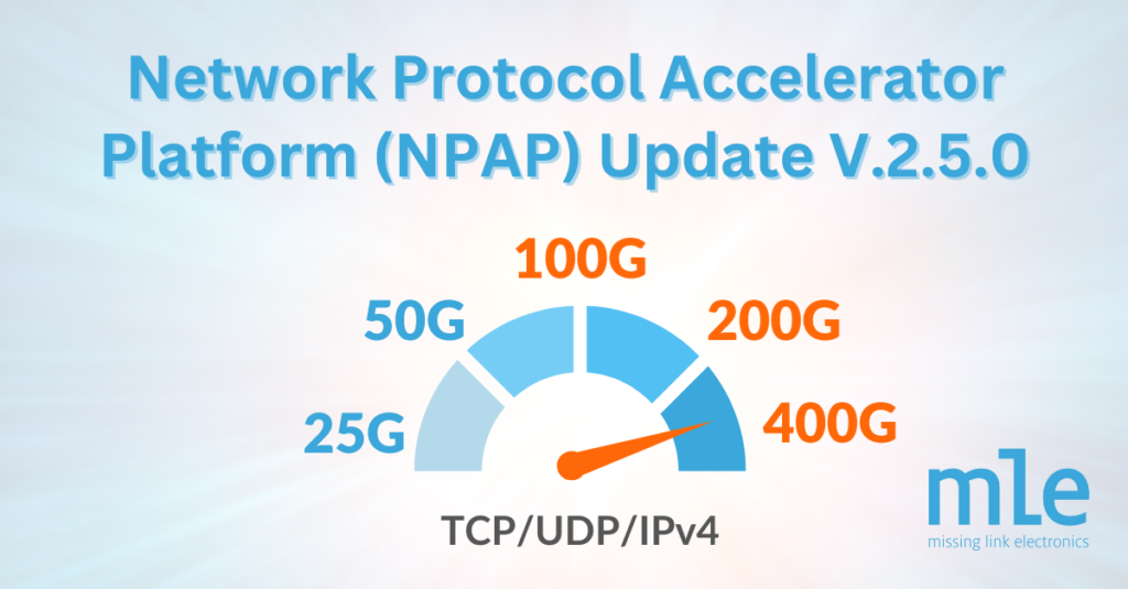
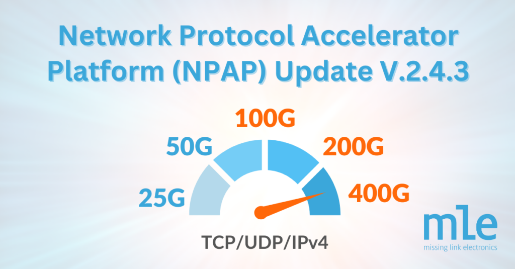
NPAP is the TCP/UDP/IP Full Accelerator from Fraunhofer HHI which enjoys production use in FPGA applications for automotive, industrial, medical, robotics, test & measurement and wired/wireless communications.
Newly introduced features include built-in diagnostics plus functionality to emulate Network Impairment.
Also added was support for the new Agilex 5E FPGA devices from Altera where MLE NPAP integrates with the GTS Ethernet Intel® FPGA Hard IP.
PCO, an Excelitas Technologies® Corp. brand, is a leading specialist and Pioneer in Cameras and Optoelectronics with more than 30 years of expert knowledge and experience of developing and manufacturing high-end imaging systems. The company’s cutting edge sCMOS and high-speed cameras are used in scientific and industrial research, automotive testing, quality control, metrology and a large variety of other applications all over the world.
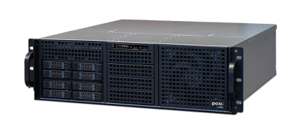
The pco.hsr 8×25 CLHS Image Recorder is equipped with a high-performance SSD tray, providing fast data storage with a capacity of up to 8 TB. It supports the simultaneous connection of 1 to 8 cameras and features a 25G Ethernet connection for efficient data transfer to a PC. The system offers flexible recording modes, including Record, Pause, Play, and Circular Buffer Recording, ensuring versatile operation for various applications.
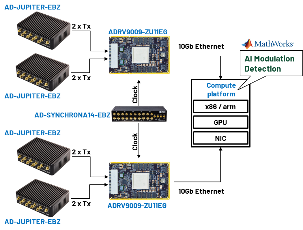
At Embedded World 2025 in Nuremberg Exhibition from March 11-13 in Nuremberg, Germany, Analog Devices (ADI: Hall 4A: Stand 360) and Missing Link Electronics (MLE: Hall 5: Stand 140) will be sharing solutions that are redefining high-speed Ethernet connectivity. Together, they are paving the way for the next generation of embedded applications across various markets ranging from automotive to industrial automation to IoT.
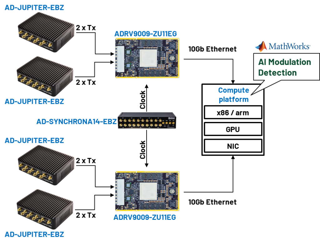
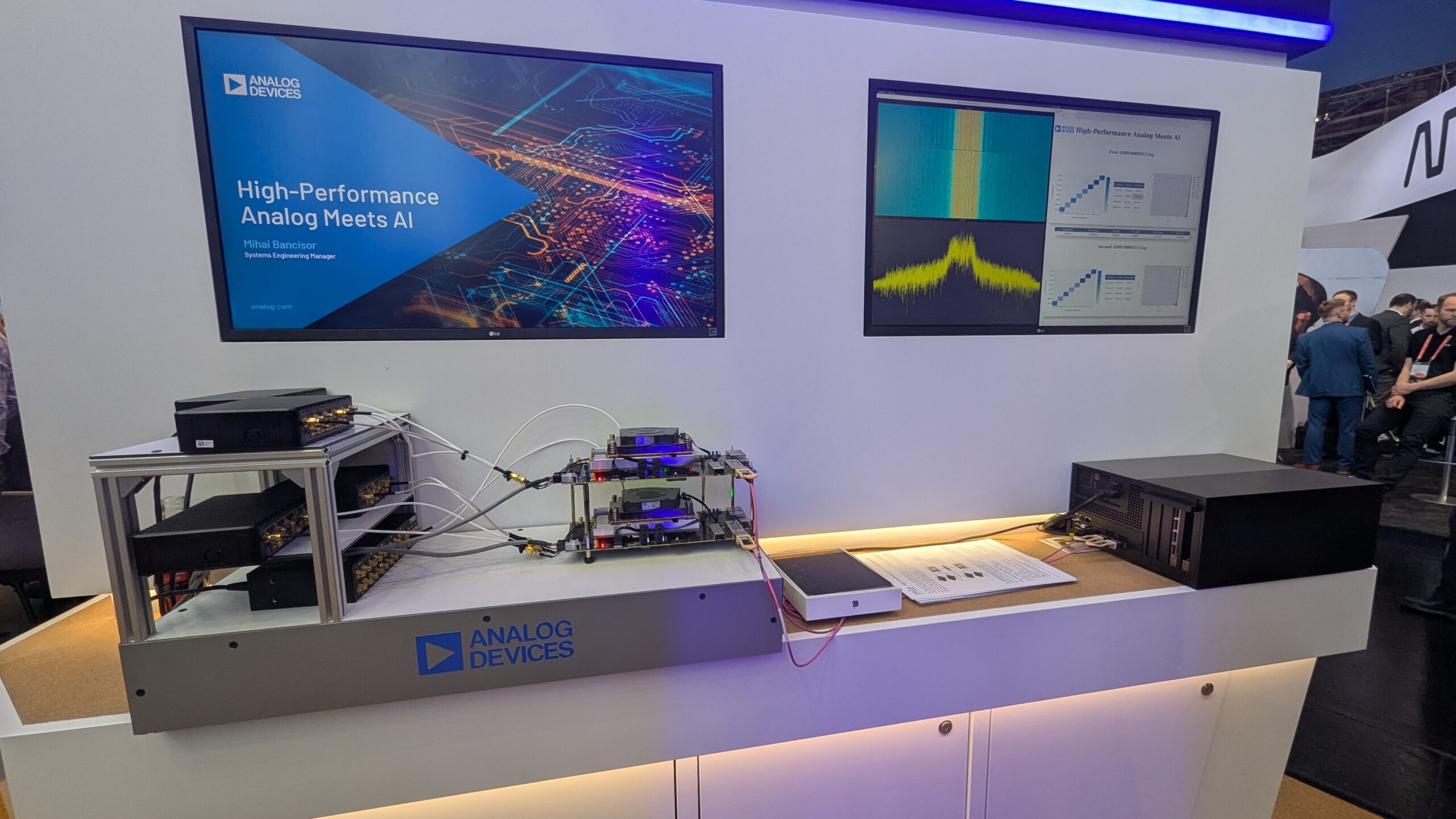
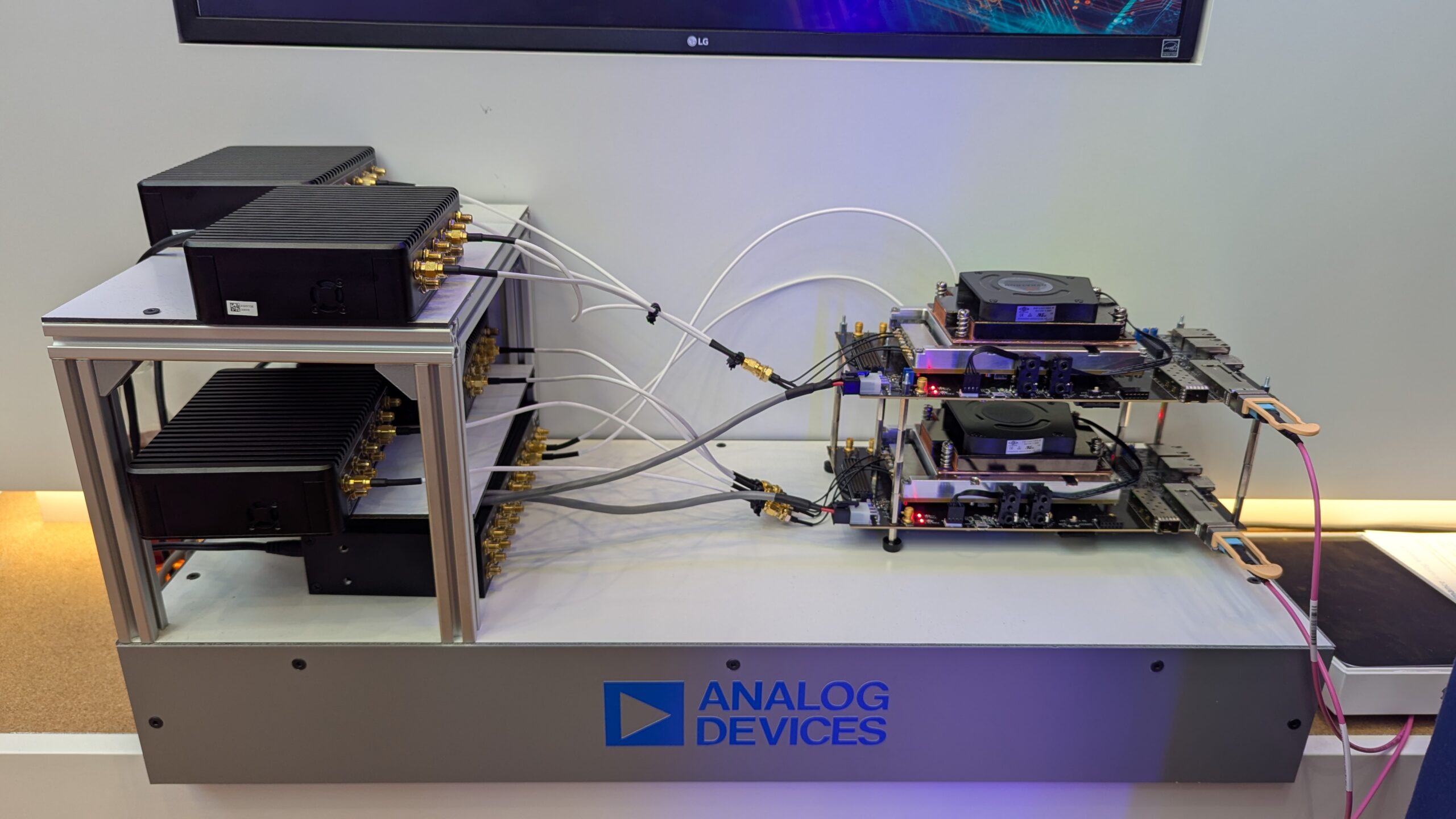
Mark your calendar to make a stop at the ADI booth to see the “High-Performance Analog Meets AI” demo. This demo dives into the shift from traditional signal processing to AI-driven flows and speaks to the trend of extracting data from high-performance, high-data-rate analog signal chains for AI model training and real-time inference.
The demo shows how ADI’s data extraction framework, built on top of open-source software, open-source FPGA infrastructure, and scalable host-side data management flows, can be used in conjunction with ADI’s high-performance transceivers and converters to streamline the development and deployment of AI-capable and intelligent edge systems.
MLE helps ADI implement Corundum – an open-source, high-performance FPGA-based NIC and platform – on the ADRV9009-ZU11EG System on Module (see ADRV9009-ZU11EG RF-SOM Hardware Overview). Via Linux NAPI, the standard open source Linux network stack, data is captured in system memory and then streamed to the Nvidia IGX/Host PC for AI processing.
Learn more about how MLE enables high performance analog for AI processing and at ADI’s EZ Blog.
High-performance data extraction architecture for AI model training and real-time inference in high-data-rate analog signal chains
MLE helps ADI implement Corundum on the ADRV9009-ZU11EG System on Module
Auto/TSN enables Software-Defined Vehicles (SDV) and zonal architectures by virtualizing industry-standard automotive such as CAN, LIN, or CSI-2 for transport over in-vehicle network “backbones”.
Auto/RPS is MLE’s FPGA-based Rapid Prototyping System (RPS) catering to the specific needs of automotive engineers designing next-generation Zone Based Architectures. MLE Auto/RPS enables automotive system engineers to design and to validate software-defined vehicle (SDV) functions along with MLE Auto/TSN in-vehicle networking.
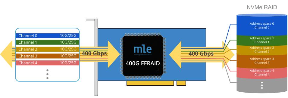
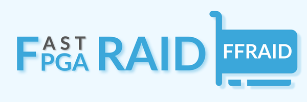
MLE Fast FPGA RAID (FFRAID) is a fast and FPGA-based NVMe RAID solution that can transfer bulky data from multiple sensors to a RAID of NVMe SSDs at speeds up to 400 Gbps. The FFRAID implements a channel-based architecture, supports data-in-motion pre- and post-processing and is highly scalable with regards to bandwidth and recording capacity.
Altera, Arrow and MLE have worked together to migrate MQNIC, an FPGA-based Network Interface Card (NIC) from the open source Corundum.io project to Altera Agilex 5E on the Arrow AXE5 Eagle Development Platform.
High Performance Analog Meets AI
📍Hall 1, booth #1-301
Analog Devices and MLE will be sharing solutions that are redefining high-speed Ethernet connectivity. Together, they are paving the way for the next generation of embedded applications across various markets ranging from automotive to industrial automation to IoT.
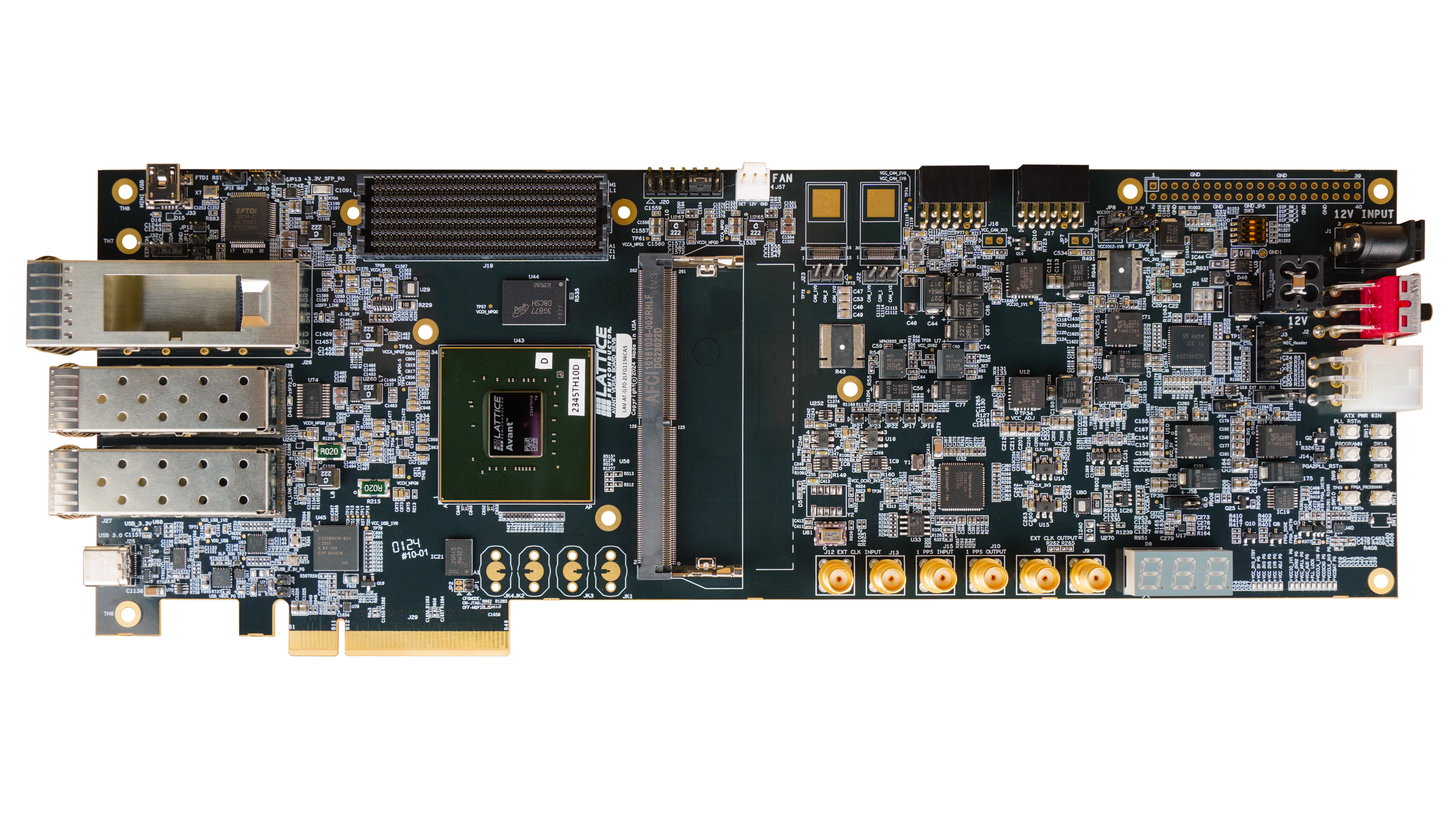
Lattice and MLE have worked together to migrate MQNIC, an FPGA-based Network Interface Card (NIC) from the open source Corundum.io project to Lattice Avant-G and Avant-X FPGAs on the Lattice Avant-G/X Versa Board.
Accelerated TCP/IP for High-Speed Camera Connectivity
📍Hall 3A, booth #3A-135
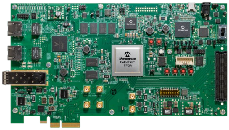
NPAP, the TCP/IP Full Accelerator from Fraunhofer HHI, provides TCP connectivity in accordance with the GigE Vision standard. Microchip has worked with MLE to integrate and to optimize MLE NPAP for PolarFire and PolarFire SoC, suitable for next-generation camera products.
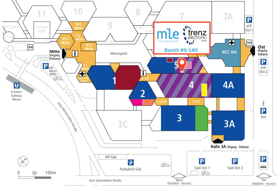
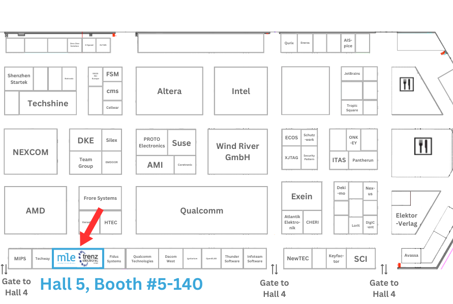
Trade Show Information
Date: March 11-13, 2025
Location: Nuremberg Convention Center, Nuremberg, Germany
Booth: Hall 5 #5-140
Visit us at booth #5-140 and talk with our FPGA experts to learn about how to accelerate your industrial network connectivity with a “shift-left approach”!
MLE’s Network Protocol Accelerator Platform (NPAP) runs the entire TCP/UDP/IPv4 protocol stack in a digital circuit, i.e. FPGA or ASIC. This means NPAP must meet some challenging combinations of Your requirements:
First (and most important of all), NPAP must be compatible and fully interoperable with the many TCP/UDP/IP software stacks in use today
Second, users expect outstanding performance: High throughput (close to line rate) and low latency (in form of short Round-Trip Times)
Resource efficiency comes next: This means avoiding “FPGA Bloat” as well as options to tune Rx and Tx buffer sizes
Then, users want us to support leading FPGA vendors and device families with their many different high-speed transceivers and Ethernet subsystems
And last, a clean and affordable license model that makes sense even for low unit volume applications such as in Test & Measurement
Over the years, MLE’s engineering team has invested significantly in NPAP’s test automation. CI (continuous integration) tools such as Gitlab integrating Pytest for simulation and hardware test cases have enabled us to run the TCP/IP stack on many different FPGA boards, to interact with different software stacks such as the many versions in the open source Linux kernel, Microsoft® Windows with its many flavors, kernel bypass implementations such as AMD SolarFlare® Onload or Nvidia® Mellanox Messaging Accelerator (VMA), for example.
One key feature to be FPGA resource efficient is the underlying 128 bit wide dataflow architecture, as this balances throughput, FPGA clock speeds and avoids “FPGA Bloat”. Other features include options for QoS (Quality-of-Service) to prioritize some TCP streams over others and means for asymmetric buffer management.
We have put special focus on cornercases which impact performance, such as Bit Errors on the wire which cause TCP Re-Transmissions which, again, cause the net throughput to drop.
An (optional) Bit Error Insertion module facilitates Your integration and testing for “not so standard” Ethernet links: Over the years we have seen systems using very low power PHYs, multiple slip-rings, “special” connectors, and such, and wanted everything just to work as much as our customers!
Thanks to the great enablement from our FPGA partners, we have always been able to start migration and testing once new FPGA hardware enters the market.
Today, MLE NPAP runs on (almost) all AMD devices starting from 7-series up to Versal (with clear plans for Versal Gen 2), and on many of those AMD Alveo cards, too.
MLE NPAP is regularly tested for Microchip PolarFire because this is important to our customers from the low-power, cost-optimized world of FPGA based cameras and computer vision.
If you have been a licensee of MLE NPAP who is interested in upgrading to the latest latest Version 2.4.3, or if your new project can benefit from reliable TCP/UDP/IP connectivity, please contact your MLE sales representative.


