Please fill in the form below, so we can support you in your request.

    X
    CONTACT MLE
    CONTACT MLE
    Please fill in the form and your requirements below, and our team will contact you soon.

      X
      CONTACT MLE

      MLE Showcases High-Bandwidth Low-Latency Robotic Connectivity for Physical AI at AMD 2026 EMEA Embedded AI Workshop
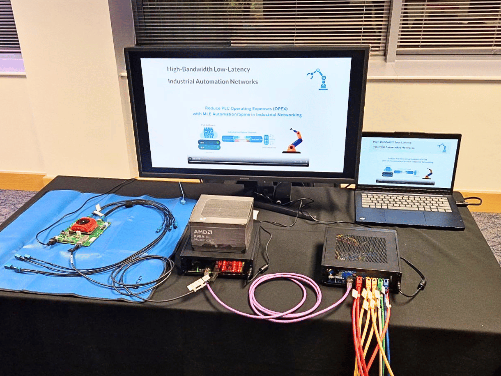
      MLE High-Bandwidth Low-Latency Robotic Connectivity_

      At AMD’s 2026 EMEA Embedded AI Workshop on November 3-4 at AMD Dublin, Ireland, MLE presented the newest robotic connectivity technology – the High-Speed Low-latency Connect for Robots (Robo/Spine) – with AMD Kria AI Solutions.

      Next generation robotic manipulation systems will be defined not only by better Physical AI algorithms, but by a better balance between centralized compute and local intelligence, and by better flexibility to partition control, communication, sensing, and local processing under real physical constraints. Therefore, solutions such as hand-mounted cameras require that high-bandwidth data streams and real-time sensing & motion control traffic can co-exist.

      Converged, Bi-Directional Real-Time Robotic Connectivity

      MLE Robo/Spine provides high-bandwidth low-latency connectivity converging various network protocols (eg. PCIe, EtherCAT, MIPI, GMSL…etc.) for deterministic real-time control with communication, sensing, and local intelligence in bi-direction within a tight size, weight, power and cost envelope. This solution delivers reliable data transports for connectivity between Sensor Plane, Actuator Plane and Decision Plane – scalable, flexible, fast, safe, secure, always on-time and open – because MLE combines open standards with data-in-motion processing and hardware acceleration of industry-standard protocol stacks.

      With Robo/Spine, MLE removes complex data-in-motion bottlenecks with deterministic, ultra-low-latency hardware pipelines where latency and jitter is measured in nanoseconds. Tunneling, the concept of transporting one protocol over another protocol, adds a layer of network virtualization and, thereby, a layer of functional safety and security. 
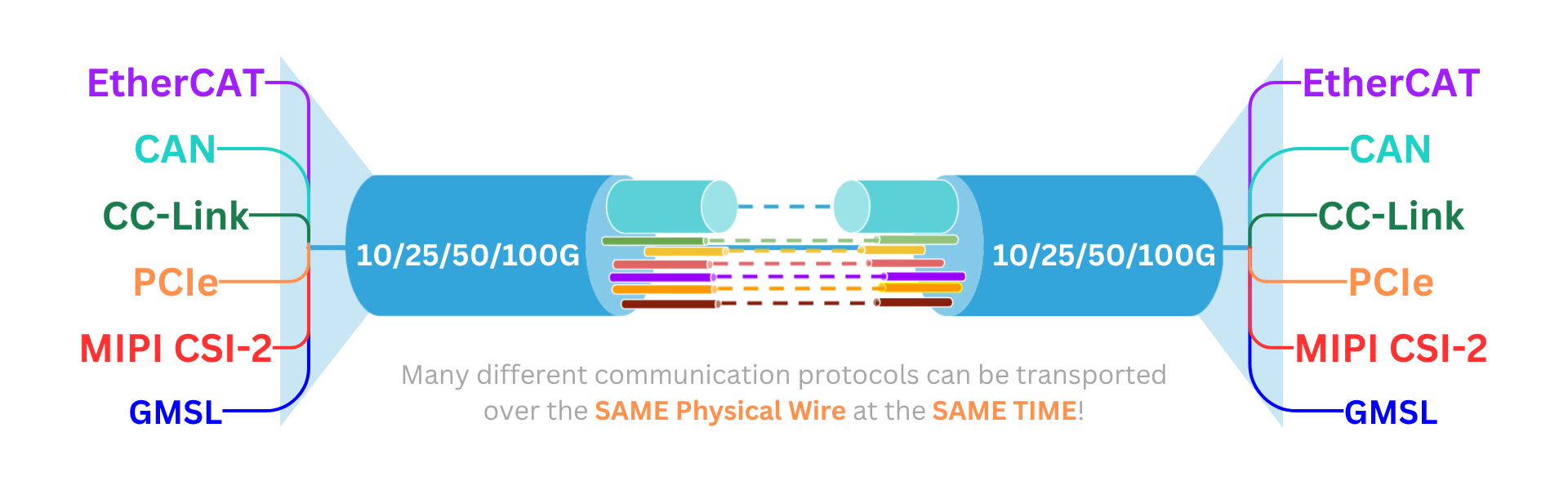
      MLE Humanoid Robot Networks_v2

      Key Features

      • Scalable from 100 Mbps to 100 Gbps
      • Agnostic to physical layer, supports fiber, copper, SPE – regain control of your BoM
      • Bridging and/or Tunneling of protocols like PCIe, EtherCAT, Profinet, Ethernet, GMSL, RS485, CAN, CAN-FD, CC-Link IE TSN, etc.
      • Hardware accelerated real-time, deterministic transport with Ultra Low Latency less than 1 microsecond
      • Reliable transports via RDMA, TCP or RRRRP over IPv4
      • Scalable IPv4 addressing from individual robott to entire fleets
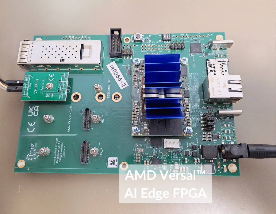
      MLE NVMe Fast FPGA RAID Now Supports Trenz TE0955 Starter Kit for AMD Versal™ AI Edge

      MLE’s NVMe Fast FPGA RAID (NVMe FFRAID) now supports Trenz Electronic’s new TE0955 Starter Kit as a comprehensive FPGA Full System Stack for AMD Versal™ AI Edge adaptive SoC, bringing high-bandwidth, deterministic PCIe Gen4 solid-state drive (SSD) mass storage to embedded systems—without requiring deep FPGA design expertise.

      Solving the Edge Storage and Memory Bottlenecks

      Next-generation edge AI, robotics, and vision platforms ingest massive volumes of high-resolution sensor streams. Logging or buffering that raw data reliably without overloading the host CPU is one of the toughest challenges in embedded design. Traditionally, integrating PCIe Gen4 physical layers and complex NVMe protocol logic means dealing with steep learning curves, heavy OS driver overhead, and unpredictable integration delays.

      NVMe FFRAID Verification & Performance Highlights

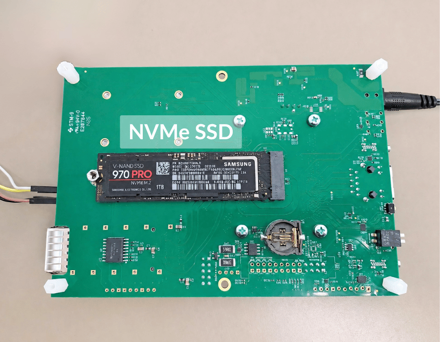
      MLE implemented our NVMe FFRAID on the Trenz Electronic TE0955 Starter Kit. This combination delivers line-rate read and write performance for AMD Versal™ AI Edge Adaptive SoC:

      • 16 GT/s Transfer Rate: Validated seamless communication with a commercial-off-the-shelf (COTS) PCIe Gen4 x4 NVMe SSD.
      • Full Protocol Offload: The NVMe protocol stack and DMA data paths run completely within the AMD Versal™ AI Edge programmable logic, offloading the scalar Arm® processor cores for critical application software.
      • Better Memory Efficiency: Unlike processor-based approaches that waste DRAM on OS buffers and byte-padding, the FPGA implementation processes data in motion using dedicated on-chip registers and Block RAM. This enables zero-copy streaming directly to the SSD without intermediate memory hops, drastically reducing external RAM requirements and shielding projects from volatile memory supply constraints.

      De-Risking System Design

      As Premier Members of the AMD Embedded Partner Program, MLE and Trenz focus on reducing technical risk for system architects. By delivering a pre-verified storage pipeline directly on Trenz’s production-ready FPGA System-on-Module (SoM), development teams can skip low-level physical interface troubleshooting, build working prototypes immediately, and accelerate their product rollouts.

      Getting Started

      The verified NVMe FFRAID for the Trenz TE0955 Starter Kit is available now. MLE and Trenz also provide design and manufacturing services to help you customize carrier boards and optimize high-speed data pipelines for your specific production requirements.

      Quickly Build and Validate Your FPGA Design on TE0955 with NVMe FFRAID

      SoC/ASIC Verification at Many-Hundred Gbps

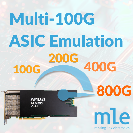
      Multi-100G ASIC Design Verification via Cost-Effective Emulation Platforms

      Applications of Agentic AI drive chipmakers to boost network and storage interfaces to many hundred Gbps. However, today’s ASIC and SoC emulation systems still clock below 100 MHz. Thus, emulating a modern 800 Gig Ethernet subsystem results in bloated logic with 8,000 (eight thousand) bit-wide internal busses – which is highly inefficient and slows down time-to-market.

      Therefore, MLE has created a “missing link” between so-called Hardware-in-the-Loop (HiL) verification and RTL simulation. Originally designed-for as MLE’s in-house verification methodology, this approach combines:

      • off-the-shelf FPGA cards (with over 1,600 Gbps I/O bandwidth),
      • MLE accelerator IP for network protocols (TCP / UDP / IPv4),
      • MLE accelerator IP for storage protocols (NVMe / PCIe),
      • open-source “gateware” and software, and
      • state-of-the-art RTL simulators with FLI/PLI.

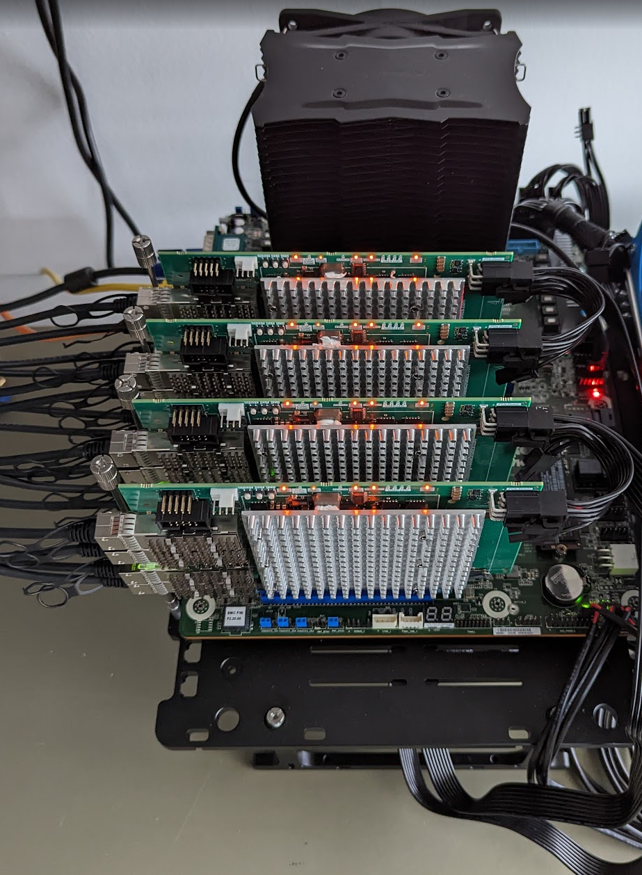
      Emulation now runs At-Speed: One or more FPGA Cards are connected to off-the-shelf servers which stimulate and stress-test the “real-life” behaviour and timing of network and storage protocols in the DUT. 

      MLE SoC/ASIC Emulator Setup

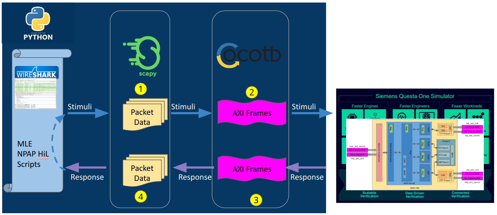
      Critical portions of the protocol traffic are recorded in standard formats such as Wireshark. Full design visibility into the inner workings of your chip – if needed even at clock-cycle accuracy – is provided by replaying these recordings in the RTL simulator via “cocotb”, the open source coroutine-based co-simulation testbench environment for verifying VHDL and SystemVerilog RTL using Python https://www.cocotb.org/ .

      MLE High-Speed Networking ASIC Emulation

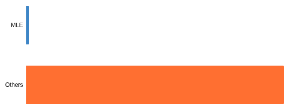
      This shortens your engineering turn-around time in the crucial verification phase towards tape-out and it significantly reduces implementation efforts for a proper testbench. Plus, this gives you a much higher test coverage over time: Such a HiL can process 100 Terabytes of test data within 20 minutes, while an emulator needs more than a week!

      Comparison of Verification Turn-Around Time Between MLE HiL Methodology And Others
      Comparison of Verification Turn-Around Time Between MLE HiL Methodology And Others (Shorter is Better)

      Looking for High-Speed Networking/NVMe ASIC or FPGA SoC Design Verification?

      John Ousterhout: “TCP is Dead!” at AI Engineer World’s Fair

      John Ousterhout, Stanford Professor and author of “A Philosophy of Software Design”, turns our attention to the evolving nature of AI networking workloads and why traditional protocols like TCP and RDMA are becoming bottlenecks in modern data center environments!

      The Shift in Workloads

      Historical context:

      AI traffic was dominated by massive, long-running transfers (gigabytes of gradients), where throughput was the primary metric.

      Modern AI:

      Workloads, especially inference and agentic applications, now rely on frequent, small coordination messages (e.g., KV cache lookups, barrier synchronization). These small messages are highly sensitive to latency. The Bottleneck: When small synchronization messages are mixed with large traffic, they get trapped in queues (caused by incast), significantly increasing 99th percentile (tail) latency. This causes GPUs to sit idle, wasting expensive compute resources.

      Why Legacy Protocols Struggle:

      Sender-Driven Congestion Control: TCP and RDMA rely on the sender to detect congestion, often via packet drops or delayed signals from switches. This process is inherently reactive and oscillates, leading to unstable performance.

      Byte Stream Model:

      These protocols view data as an opaque stream of bytes rather than discrete messages, making it difficult to prioritize short, critical tasks.

      The Homa Solution

      John introduces Homa, a clean-slate transport protocol designed for data centers:

      Message-Based:

      Unlike byte streams, Homa understands message boundaries, allowing it to predict traffic and prioritize short messages using Shortest Remaining Processing Time (SRPT).

      Receiver-Driven:

      The receiver controls the flow by issuing grants to senders, effectively managing congestion before it occurs at the switch.

      Priority Queues:

      Homa leverages the multiple hardware queues already present in modern switches to bypass long, queued traffic with low-latency short messages.

      Performance Results:

      Benchmarks show Homa can reduce tail latency for short messages by over 10x compared to TCP, while simultaneously improving performance for large messages.

      Learn More about HOMA Technology?

      MLE NPAP Network Accelerators Now Supports Trenz TE0955 with AMD Versal™ Adaptive SoCs for Physical AI Connectivity

      MLE NPAP Network Accelerators Now Supports The Trenz TE0955 with AMD Versal Adaptive SoCs for Physical AI Connectivity

      Your AI models are ready for prime time, but legacy bus architectures and software-based protocol stacks are choking your system with millisecond lag and heavy CPU overhead?

      In industrial control automation, software stacks simply cannot keep pace with arrays of high-bandwidth sensors arrays.

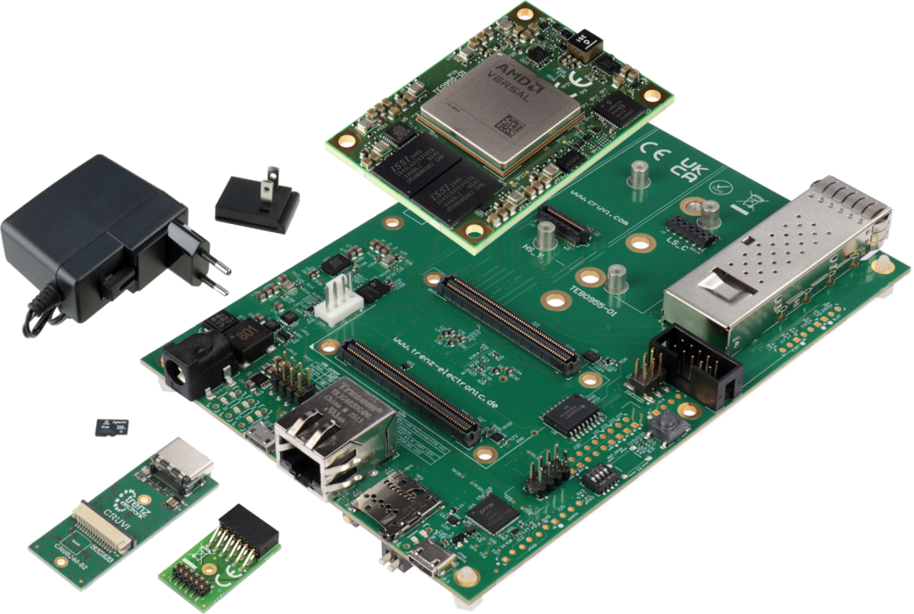
      Use MLE NPAP TCP/UDP/IPv4 Accelerators on AMD Versal Adaptive SoCs like Trenz TE0955 Starter Kit for reliable ultra-low-latency, high-speed camera connect to your Physical AI.

      By accelerating these slow software protocol stacks, MLE replaces complex data-in-motion bottlenecks with our deterministic, ultra-low-latency hardware pipelines where latency and jitters are measured in nanoseconds.

      MLE NPAP on Trenz TE0955 with AMD Versal™ AI Edge VE2302 supports 1 / 2.5 / 5 / 10 / 25 / 40 / 50 / 100 Gigabit Ethernet to provide a reliable high-bandwidth cameras or sensors for Physical AI Connectivity.

      Trenz TE0955 with AMD Versal™ AI Edge VE2302

      Learn more on how we achieve high-speed camera connectivity with Physical AI:

      Meet MLE at 2026 AMD Embedded Computing Summit in Frankfurt

      AMD Embedded Computing Summit 2026

      The Embedded Computing Summit 2026 will be held October 1 in Wiesbaden, Germany. MLE will be together with Partner Trenz Electronic showcasing FPGA Full System Stacks with AMD Versal.

      The Embedded Computing Summit (ECS) Global Technical Tour from AMD brings together engineers, architects, and technology leaders who are building the next generation of embedded systems.

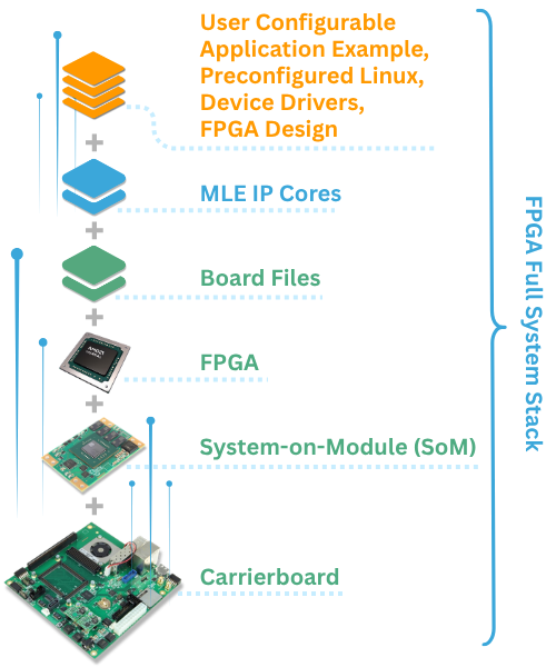
      Visit us at the ECS to learn more about how our FPGA Full System Stacks accelerate your design projects via using:

      Trenz FPGA Full System Stack composition for AMD Versal

      Date: 01 October, 2026 | 08:00-18:30

      Location: RheinMain Congress Center, Wiesbaden

      AVL Uses MLE’s NVMe Fast FPGA RAID (NVMe FFRAID) for Automotive Data Recording

      AVL List_logo

      NVMe Fast FPGA RAID (NVMe FFRAID) from Missing Link Electronics finds yet another application: AVL List uses this subsystem for accelerated data recording directly from the FPGA’s Programmable Logic (PL) to/from a Non-Volatile Memory Express (NVMe) Solid-State Drive (SSD).

      Looking for High-Speed Data Recording Solution for Automotive Applications?

      AVL List_logo

      AVL List GmbH (“AVL”), headquartered in Graz, Austria, is one of the world’s leading
      mobility technology companies for engineering, simulation, and testing in the
      automotive industry, and in other sectors such as aviation, marine, and energy. Its
      customers include leading automotive manufacturers, suppliers, and companies from
      the energy, transport, and industrial sectors.

      For more than a decade MLE has demonstrated expertise in offloading CPUs and in
      accelerating software-rich system stacks via so-called Domain-Specific Architectures. To
      implement this MLE makes heavy use of heterogeneous processing such as FPGAs
      which are programmed using C++/C/SystemC as well as VHDL and Verilog HDL for FPGA
      design. MLE is headquartered in Silicon Valley with offices in Berlin and Neu-Ulm
      Germany.

      MLE Presents “Real-Time Networking with Stanford’s HOMA Protocol” at Storage Developers Conference 2026

      SNIA Developer Conference_2026

      The Storage Developers Conference (SDC) 2026 of SNIA, the Storage and Networking Industry Alliance, will be held Sept. 28-30 in Santa Clara, CA. There, MLE will present “Real-Time Networking with Stanford’s HOMA Protocol“.

      At SDC 2023 and SDC 2024, we presented Homa, a reliable datacenter transport-layer protocol invented by John Ousterhout at Stanford University. We were able to demonstrate that Homa and TCP can co-exist in the same network “peacefully”, and how Homa can be accelerated by something similar to what Offload Engines do for TCP.

      Today, (almost) everybody’s eyes are on datacenter infrastructure and AI clusters because of the challenging Terabit line rates and the high volume numbers of network ports. Nevertheless, there are many other applications which can also benefit from Homa: 

      • Systems-of-systems such as zone-based automotive networks
      • Telecommunication core networks
      • Converged IT/OT networks in industrial automation
      • Backbones in humanoid robots
      • Sensor Open Systems Architectures in aerospace & defense

      These systems need a reliable transport-layer protocol which minimizes tail latency and optimizes infrastructure efficiency to deliver bandwidths of 10 Gbps, and more.

      Many of these systems require hard real-time behavior which – in theory – matches with Homa’s attributes of being:

      1. message-based
      2. connection-less
      3. using receiver-driven congestion control
      4. run-to-completion (SRPT)

      Time Sensitive Networking (TSN) has become the de-facto choice using IEEE standard Ethernet. TSN comes with time-synchronization, traffic shaping, reliability and resource management and works well with higher-layer protocols such as TCP.

      Hence, in our presentation this year we will share insights on how Homa can be run over TSN and, in particular, the effects of different forms of traffic shaping on Homa’s core functions. We plan to start with a refresher on Homa and then dive into architecture choices when running TSN and multiple Gbps. This is complemented by presenting “Light Rabbit” which is a cost-optimized variant of CERN’s White Rabbit high-accuracy time synchronization which utilizes programmability of modern PLLs for frequency and phase synchronization to achieve nano-second accuracy. We close by presenting first experimental results of running Homa over TSN to achieve the best of both worlds.

      Date: September 28-30, 2026

      Location: Hyatt Regency Santa Clara, Santa Clara, CA

      MLE Presents “Beyond the Bitstream: Streamlining Heterogeneous Computing with the MLE FPGA Full System Stack” at FPGA Conference 2026

      Beyond the Bitstream: Streamlining Heterogeneous Computing with the MLE FPGA Full System Stack - FPGA Conference 2026

      The FPGA Conference Europe 2026 will be held June 30 – July 2 in Munich, Germany. There,  MLE will present “Beyond the Bitstream: Streamlining Heterogeneous Computing with the MLE FPGA Full System Stack.”

      As the demand for domain-specific architectures grows, FPGAs have become essential for offloading compute-intensive tasks in networking, storage, and automotive sectors. However, the “Integration Gap”—the months of engineering effort required to build reliable PCIe/DMA infrastructure, kernel drivers, and memory management—often acts as a barrier to entry.

      This presentation introduces the Missing Link Electronics (MLE) FPGA Full System Stack (FFSS), a pre-validated, cross-platform framework designed to eliminate architectural “plumbing” and accelerate application-specific development.

      Date: Thursday July 2rd, 2026

      Track Architecture 2:20pm-3:00pm CEST

      Location: Hotel NH München East Conference Center, Munich, Germany

      Join MLE at FPGA Conference 2026 and discover how our FPGA Full System Stacks de-risk design process, rapidly validate your prototypes, and accelerate your time-to-market!